1. Interactive PCB Concept
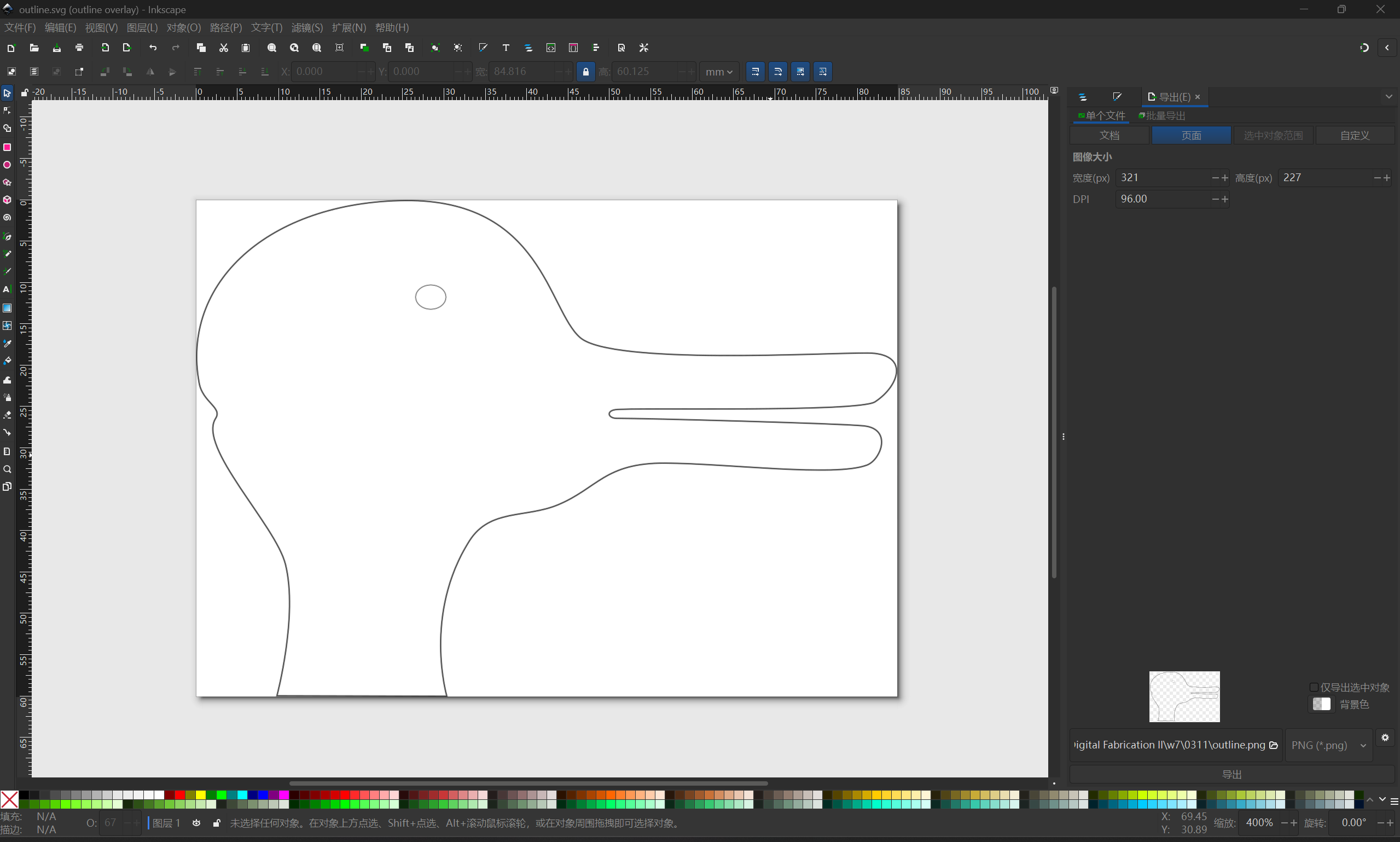
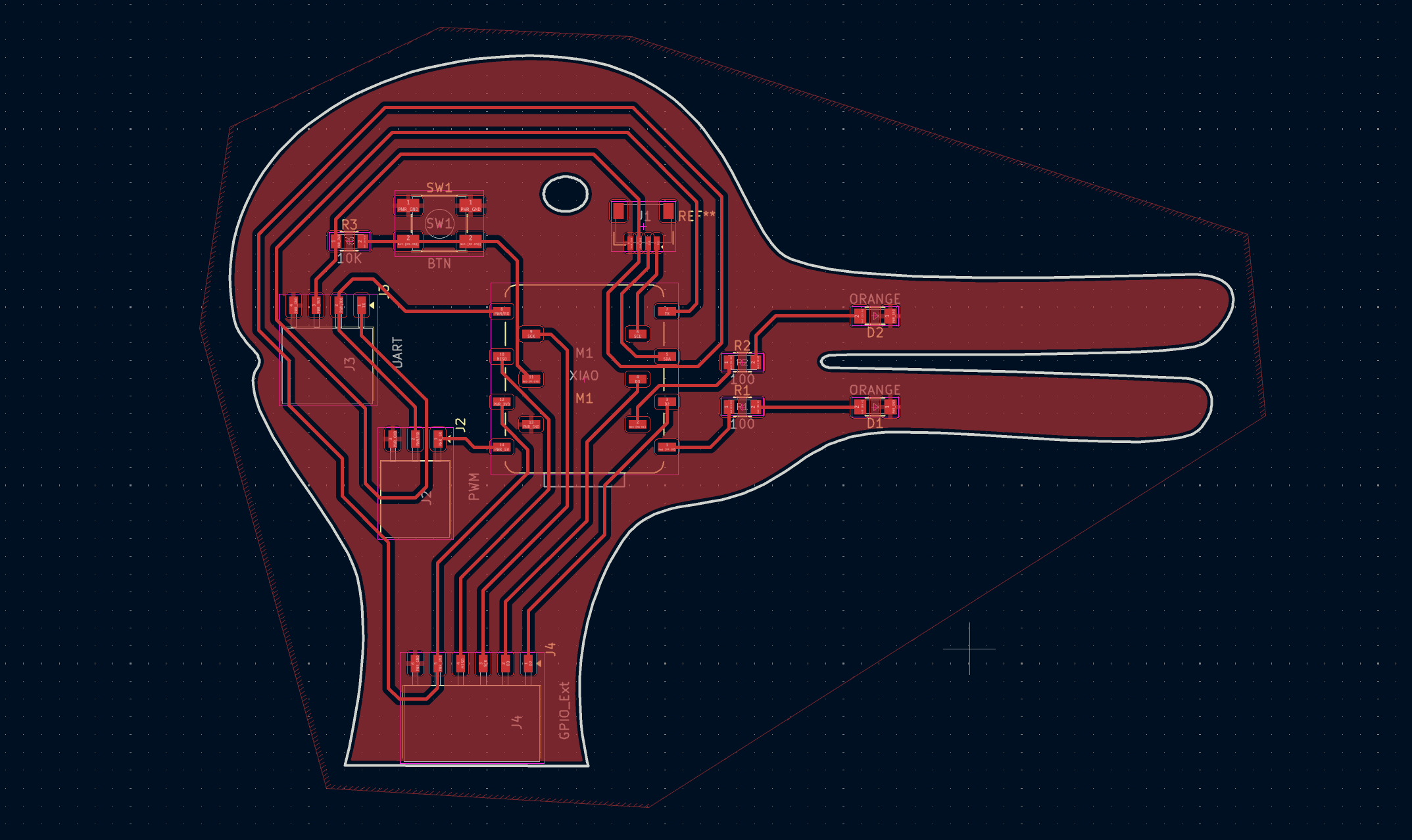
This is the first time I have tried to design a circuit board, and I spent a long time thinking about what kind of outline to create. In the end, I decided to design a custom-shaped circuit board based on the famous "Wittgenstein's duck-rabbit" illusion. Rather than a traditional rectangular product, this board serves as a small interactive art installation and a personal keepsake. Because I could not place the LEDs directly as eyes due to physical cutting constraints, I arranged all the interactive components (the MCU, button, and two LEDs) neatly within the solid copper area. Learning how to design custom PCBs is incredibly useful for my future projects. I hope to continue exploring these functionalities to build more engaging interactive installations or physical games. I sketched the initial vector outline in Inkscape, ensuring it was a continuous closed path ready to serve as the PCB boundary.
2. Schematic Layout
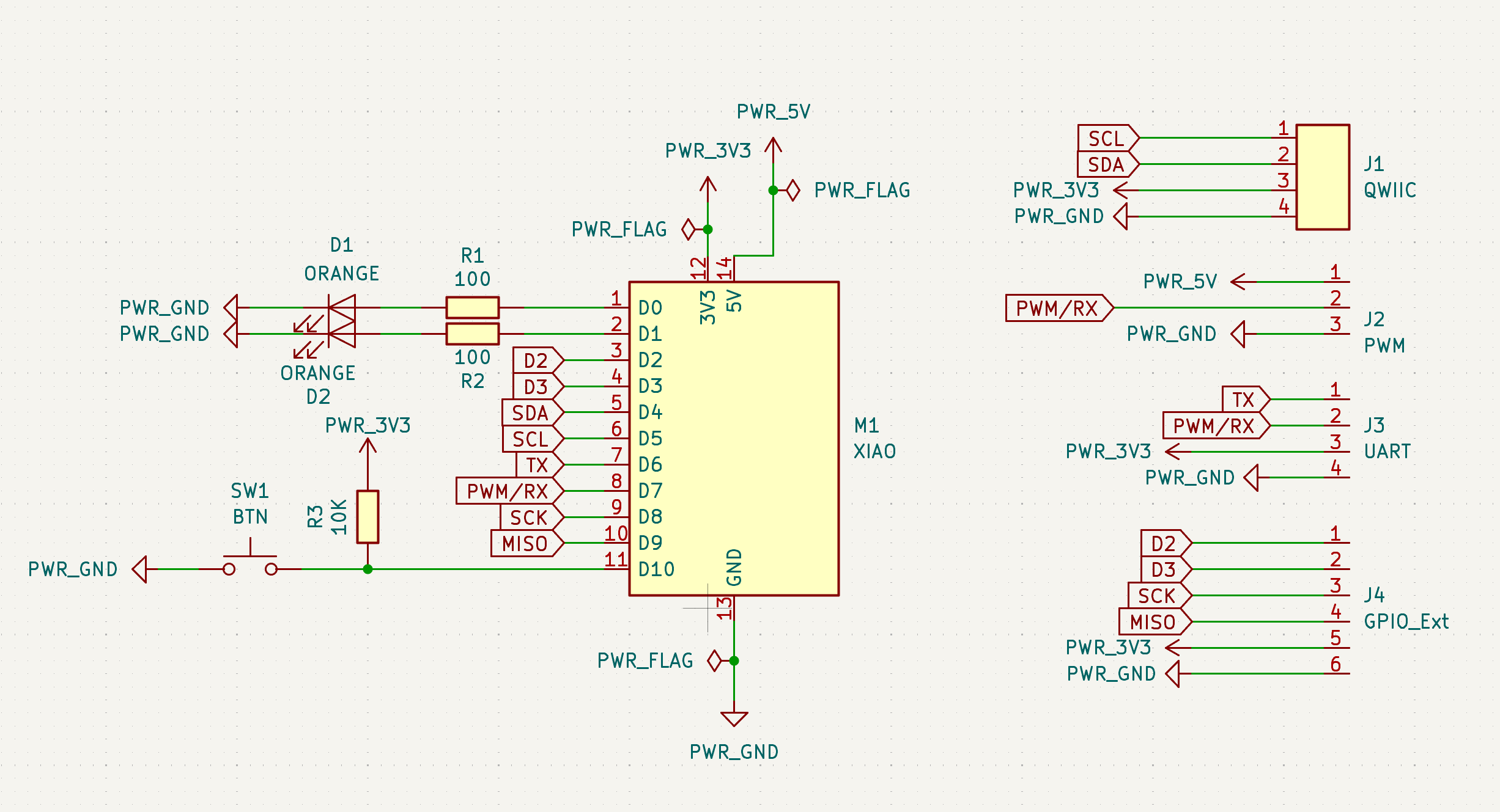
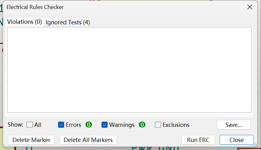
I used the Seeed XIAO RP2040 MCU symbol in the KiCad Schematic Editor to design the circuit. To meet the assignment requirements, I added two 1206 SMD Light Emitting Diodes (LEDs), each with its own 100-ohm current-limiting resistor to protect it, as well as an Omron tactile button. To ensure a stable high state when not pressed, I connected the button to a digital pin and ground with a 10k-ohm external pull-up resistor. To make it easy to add more components later, I included a horizontal SMD connector for I2C (Qwiic standard: SCL, SDA, 3V3, GND) and added a 4-pin female header for UART and a 6-pin female header (GPIO_Ext) to break out the remaining pins. Finally, I attached PWR_FLAGs to the 3.3V and GND lines to correctly define the power sources, allowing my design to pass the Electrical Rules Check (ERC) with zero errors.
3. PCB Routing
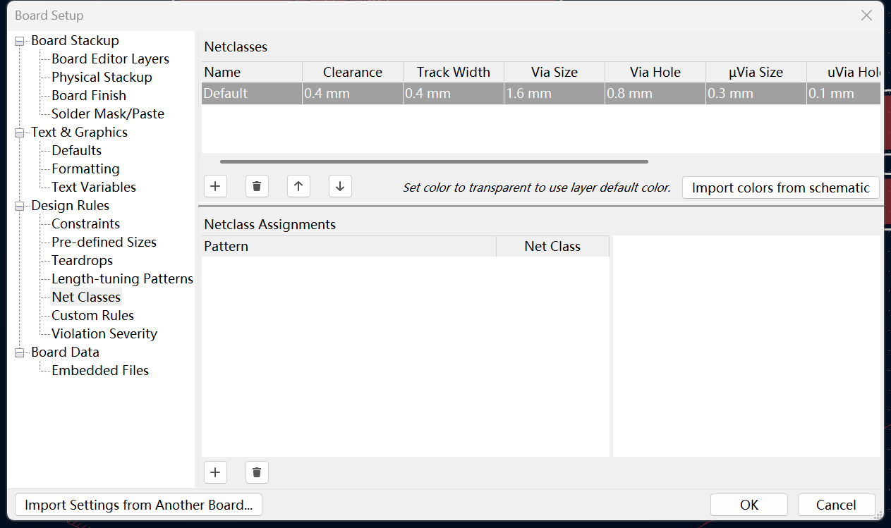
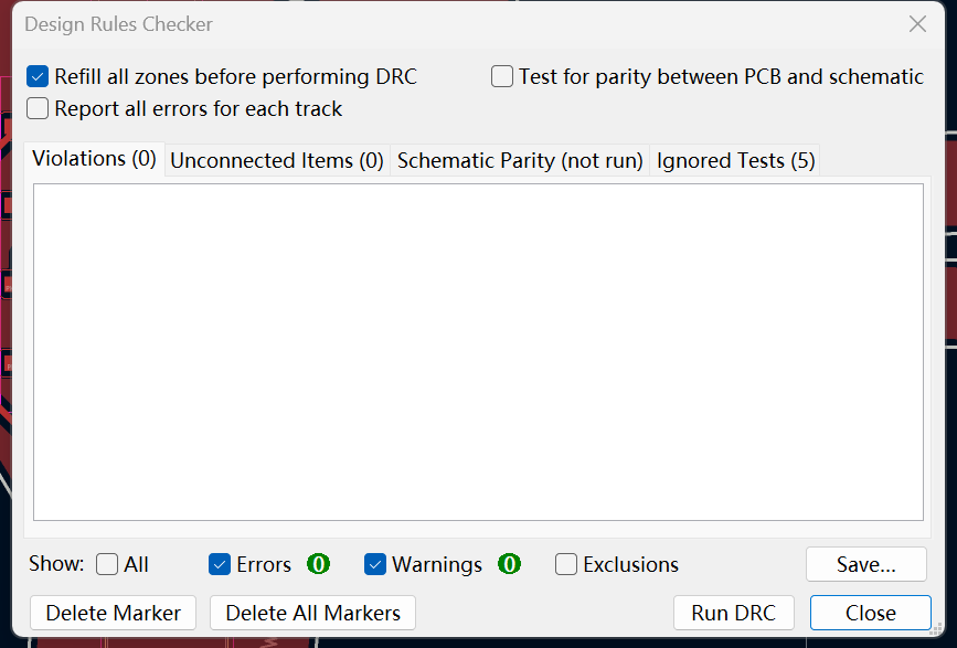
I imported the duck-rabbit SVG file into the Edge.Cuts layer to define the physical boundary. This layer tells the machine where to cut. Before routing, it was important to set the Net Classes. I set both the clearance and track width to 0.4mm. This is necessary because the Roland SRM-20 milling machine at the Fablab uses a 0.4mm tool, and traces closer or thinner than this would be destroyed. I placed the MCU, LEDs, and button on the neck area and routed all signal traces on the F.Cu (Front Copper) layer. This is the top conductive layer. Finally, I used the filled zones tool to create a GND copper pour across the entire board, which made the routing easier. The board passed the Design Rules Check (DRC).
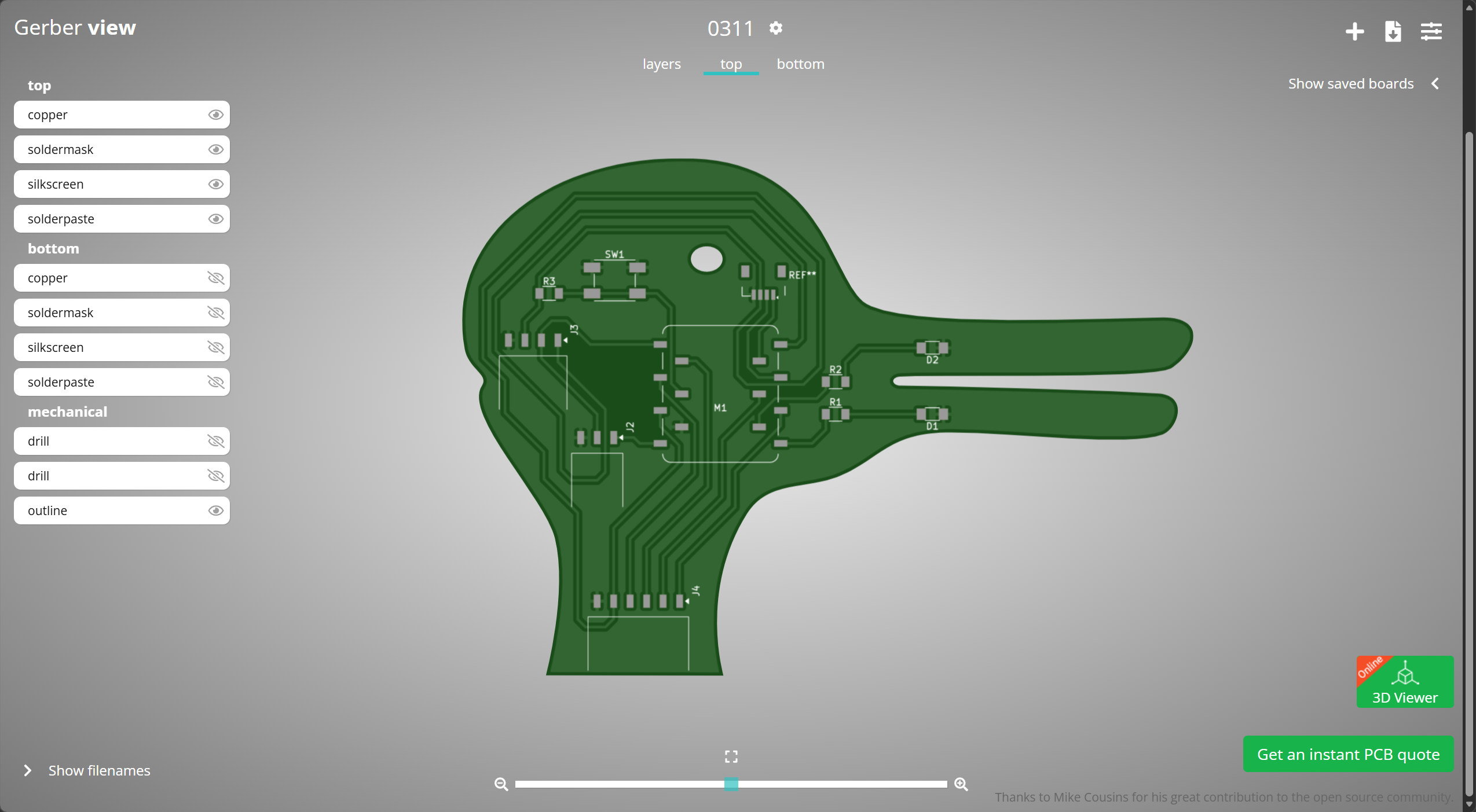
4. Manufacturing Export
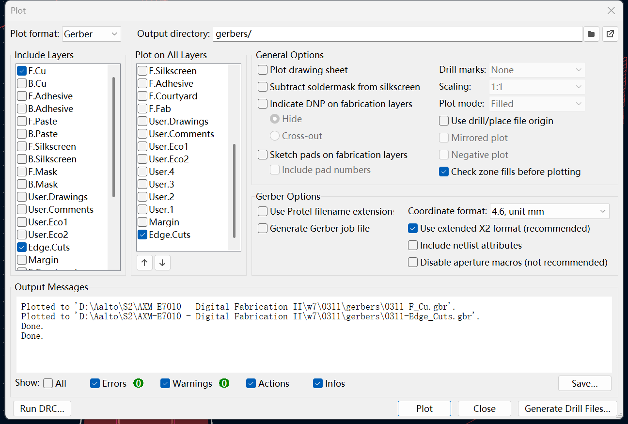
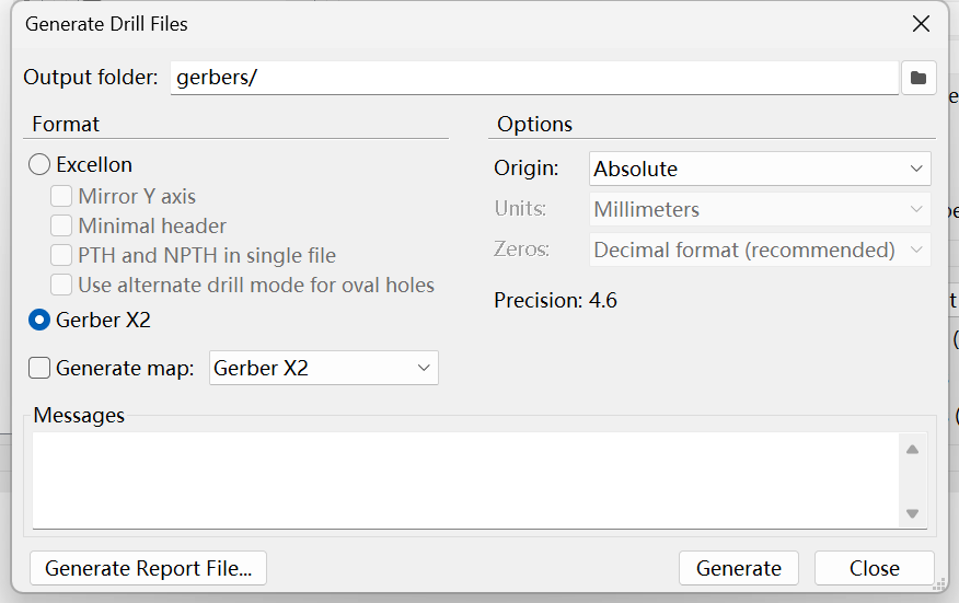
The final step was to export the board for the manufacturing process. Instead of manually plotting individual layers, I used the "Gerber to order" plugin from KiCad's Plugin and Content Manager. This automated tool generates all necessary production files—including the F.Cu layer for conductive traces, the Edge.Cuts layer for the custom duck-rabbit outline, and the required drill files—and instantly packages them into a convenient ZIP archive. This streamlined workflow is highly efficient for sending designs to external fabrication facilities like PCBWay. To verify my files, I uploaded the generated ZIP package directly to the PCBWay online viewer. The resulting 3D preview is not bad.
Download
Project Files (.zip)